|
|
|
|
DEC & ALPHA CPU's |
|
 |
 |
LSI 11/2 CPU Module |
|
This module was used as CPU
of the PDP-11/3 System. The LSI-11/2 offered 83 standard PDP11 instructions, 8 optional EIS/FIS instructions, 32 KW adressing range, MicroODT (Octal Debugging Technique on the console) and one interrupt level. |
||
| source: http://hampage.hu |
|
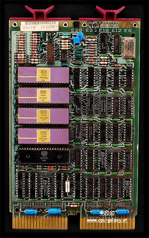
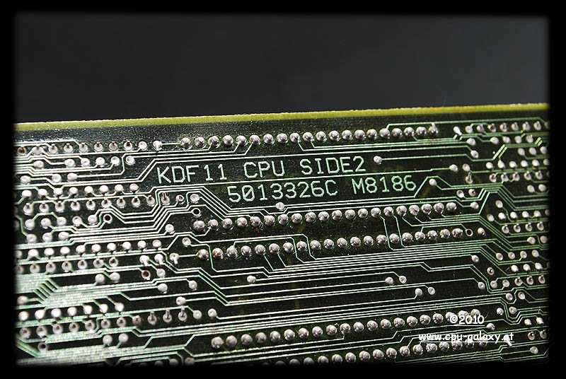
DEC M8186 11/23 CPU MODULE KDF11-A The KDF11-A
module has four 40-pin sockets for the chipset. One is for the DCF11
two-chip hybrid (21-15541AB data path and 23-001C7 control chip), one's
for the KTF11 MMU option and one's for the KEF11 floating-point option
(another two-chip carrier; the MMU must be installed to use the FPP
option). The remaining socket can be used with the CIS option, which
spans two sockets wide (so you loose the FPP). The KDF11-B has five
sockets, so there are no problems |
 |
   |
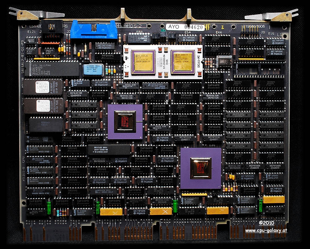 |
DEC M8190-AE KDJ11-BF CPU PDP 11/84 This PDP-11/84 CPU, M8190 or KDJ11-BF (1985), microprocessor-based J-11, was a high-end PDP, which supported advanced solutions such as memory cache (mounted on same card), the FPU on board and memory interconnect system, a communication channel between high-speed CPU and memory. The J-11 (1983) was essentially an implementation of the microprocessor in the form of PDP 11/70, with support for SMP and cache memory. The execution of floating point instructions can be accelerated by adding an optional FPU. Like its predecessor F-11. The J-11 also supported the instruction set "commercial" CIS (by adding a special microcode ROM). The J-11 is a multi-chip microprocessor, consists of two separate base unit (Control Chip and Data Chip) and a possible third unit, the FPU (FPA Floating-Point Accelerator).
Source: http://ummr.altervista.org |
||||
   |
|||||
|
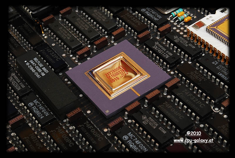
DEC KA820-AA CPU The DEC KA820-AA (1985), based on the bus VAX-BI, contains the CPU V-11 "Scorpio" clocked at 5 MHz. This processor was used in the VAX minicomputer 8250/8350 (1986). The V-11 was from a historical point of view the first implementation of the architecture in the form of microprocessor VLSI VAX. The V-11 CPU has four distinct units: the chip ROM / RAM, the integer execution unit, a unit of memory management, cache and address translation, which also acts as a I/O controller, and an accelerator for floating point operations
|
 |
||||
   |
|||||
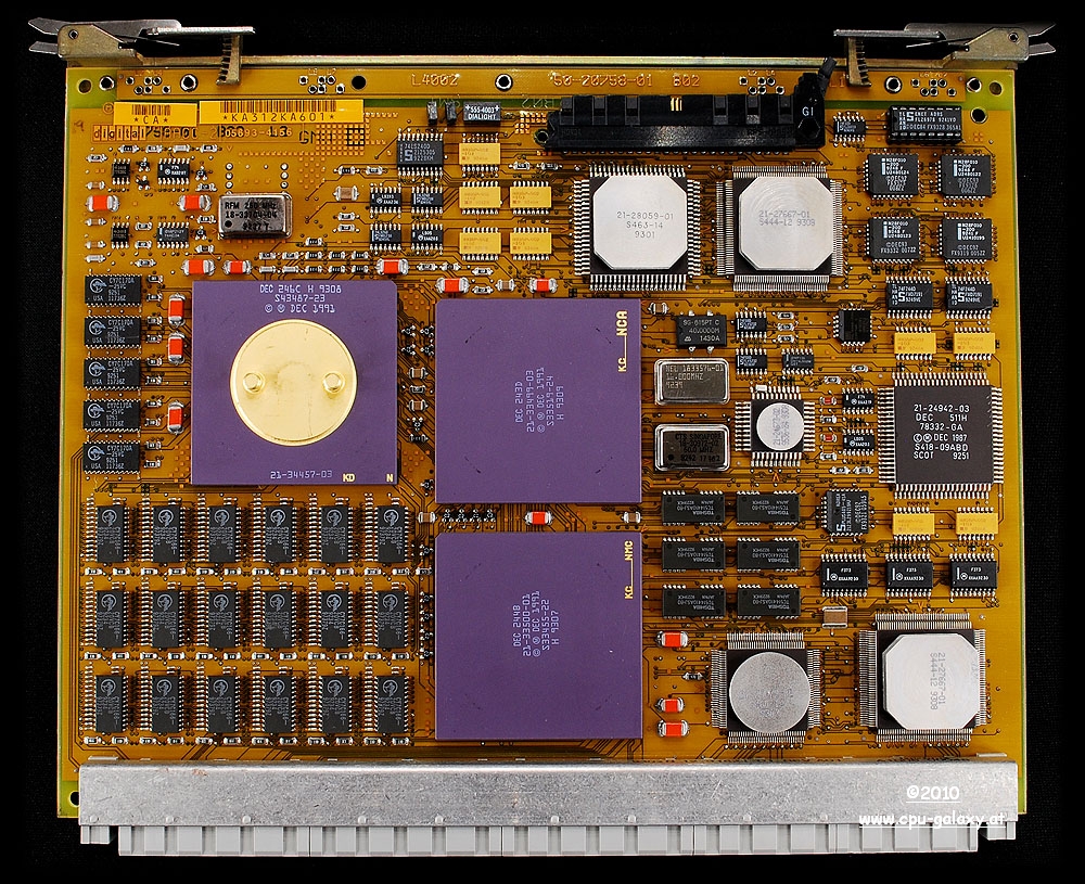 |
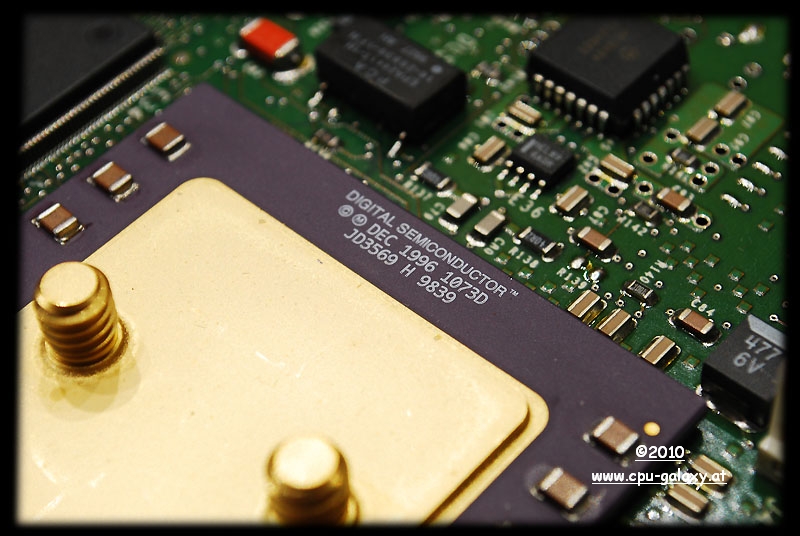
DEC KA680-AA CPU This is a processor for VAX machines 4000/M500. The board hosts a 75 MHz CPU NVAX (left, with the gold heat spreader) . The NVAX was the last step evolutionary VAX architecture, and the fastest CISC CPU available (1991). Developed in parallel with the Alpha 21064 RISC processor with similar production process, technological and human resources is widely regarded as the maximum achievable within CISC. Contains approximately 1.3 million transistors in CMOS4 process with 0.75 um, triple metallization, reduced to 0.50 um in the "Plus" version (CMOS5). As for the complexity is comparable NVAX at Intel 80486, but the performance and architectural solutions are definitely higher! This is a single processor chip (which contains both the floating point unit as the cache controller) based on macro-pipelined architecture type with branch prediction, highly optimized implementation of VAX instructions with the use offewer possible clock cycles.
Source: http://ummr.altervista.org |
||||
  |
|||||
|
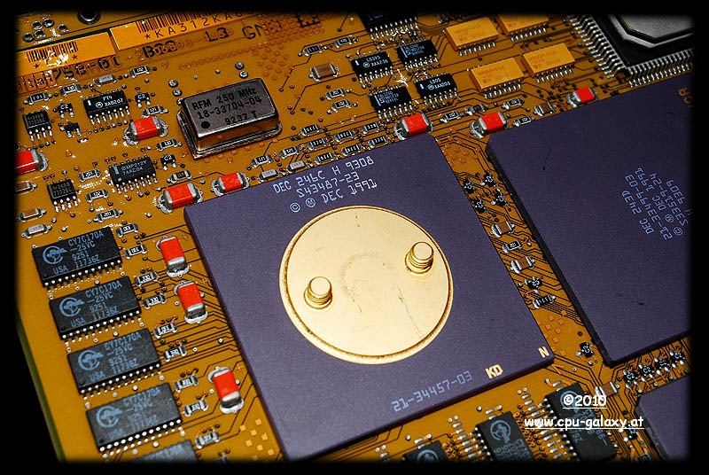
Processor Card AlphaServer 1000 4/266 This is a processor card for an AlphaServer 1000 4/266, DEC 21064 CPU clocked at 266 MHz. The AlphaServer 1000 midrange system was a single CPU based architecture EISA / PCI. One could expand the RAM up to 1 GB. The card contains the DEC chipset 21072. Source: http://ummr.altervista.org |
 |
  |
 |
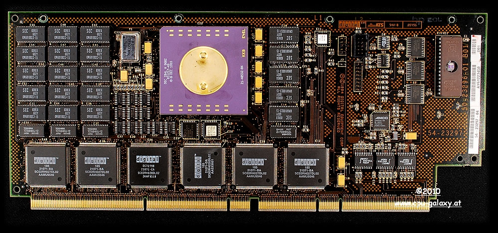
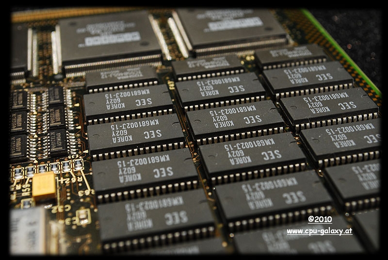
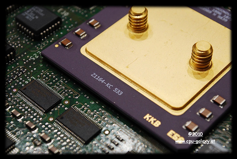
Processor Card AlphaServer 1200 5/533 CPU module Alpha 21164A 533 MHz. Contains 4 MB of L2 cache |
  |
|
Processor Card AlphaServer 21264/ 733 |

|
  |
|
|